Watch: IT Minister’s Masterclass On India’s Semiconductor Ecosystem
New Delhi:
IT Minister Ashwini Vaishnaw explained how his ministry is working to create an all-inclusive semi-conductor ecosystem in India in line with Prime Minister Narendra Modi’s “Make-in-India” vision.
In a little over four-minute-long video, the minister charts up the plan to develop a comprehensive semiconductor setup in India, complete with a talent pool of thousands and a research system encompassing over a hundred universities in the country.
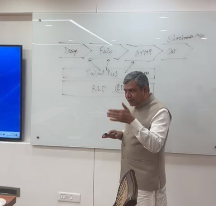
During his media interaction today after the cabinet approved three more semiconductor units, the minister laid out the plan on a whiteboard, drawing up each step with a marker in great detail.
There are four main components in the entire process – Design, fabrication, or FAB, assembly-testing-marking-packaging, or ATMP, and electronics manufacturing, or circuit,” the minister explained.
“The primary thing we are developing for this is a talent pool. The second big thing we are doing is research and development, or R&D,” he added.
What steps are being taken to augment the talent pool and for research and development? The minister explained: “The most difficult and the most expensive tools, called Electronic Design Automation, or EDA, tools, are supplied by Cadence, Synopsys, and Siemens. These are very expensive. If you go to buy one, you will have to shell out ₹ 10 crore – ₹ 15 crore for just one license. So, we have spoken to these three companies and have taken their EDA tools and given them to 104 universities in the country.”

